 A newly developed cleaning and activation process and system that both saves up front costs and provides long-term savings. The Reactive Ion Etching (RIE) is a dry etching process used in electronic and microelectronic manufacturing. This technology provides these benefits and resources:
- 1. Optimized Homogeneity by RF power split and control system designed to supply multiple electrodes with one customized RF integrated network which yields typical etching homogeneity of better than +/- 5% over 1.25 m² substrate treating area for up to 5 drawers.
- 2. A fully automatic RF tuning system (no manual control option) and a superior electrode, contact and shielding design gives a high long term process stability producing a etching rate repeatability of less than 5% from run to run
- 3. Less expensive than microelectronic etchers and more affordable that competitive systems of the same or lesser quality
- 4. An economic lab-system for prototyping and small volume production that can be customized based on application.
- 5. Fully automatic equipment with optimum plasma process components for the price of a strip down competitive system
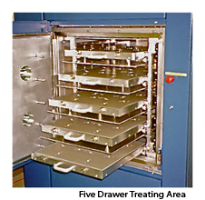
- 6. Drawer concept allows 1.25 m² substrate treating area in a compact machine with less than 1.6 m² footprint
- 7. PC based control system with graphic visualization, data logging and preset or customizable recipes to ensure process repeatability and optimum quality
- 8. Fail safe design prevents mechanical damage of components that often lead to RF supply failures of competitive etching system
Applications are for example fast and ultra high surface cleaning, surface activation, photo-resist stripping and semiconductor etching. The integrated turnkey systems are available in a variety of sizes and configurations, as well as custom systems.
Technology
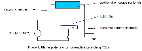
The reactive ion etching and cleaning process utilizes a planar plate reactor (see figure 1), after generating a gas atmosphere with a pressure of 10-2 to 10-1 mbar the gas discharge (plasma) is ignited by applying an radio frequency (RF) voltage.
A negative DC potential builds up automatically at the smaller electrode (substrate carrier), which is caused by the mobility of light electrons and heavy ions in the electric field. This self-bias potential usually is about 10 to a few hundred volts.
The etching effect to the substrate (wafer, PCB etc.) is the sum of at least two processes, a physical and a chemical one:
- a. Chemical etching/removal of the substrate surface or contamination by reaction with reactive gas particles generated in the plasma (plasma etching).
- b. Physical etching of the surface by transfer of direct momentum of heavy ions which are accelerated in the electric field (sputter etching)
RIE process combines the advantages of both technologies which provides high selectivity, high etching rate and isotropic etching.
Applications
 The RIE system and process is best suited for small lot production, pre-production and prototyping and provides both cleaning of surface and/or activation of surfaces.
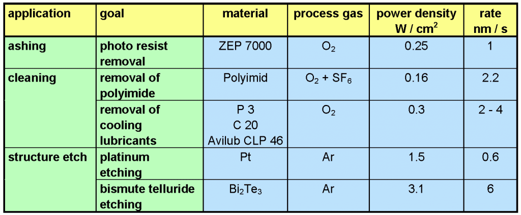
On the right is a table of processes we developed for several applications in the field of asking, cleaning and structure etching.
Here are more applications for this unique system:
Prototype or short run production of electronic and microelectronic devices
a. Laser Diodes
b. GaAs Technologies (HEMT)
c. Flip Chips
d. Transistors
e. Integrated circuitsDisc Manufacturing
a. DVD
b. CD MasteringAshing Cleaning
a. Lead Frame Cleaningb. Metal Components
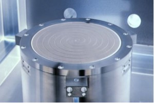
Picture 1: Electrode with Helium cooling of the substrate for high rate etching application
Systems and Components
Based on proven expertise and experience in RF technologies, AURION has developed a series of very flexible RIE systems with an outstanding cost-performance ratio. The ranges of goods include but are not limited to, three standard system sizes based on substrates, throughput and etching rates. With high capacity of up to 25 wafers (Ø 150 mm) or 20 wafers (Ø 200 mm) and despite the small footprint (max. 1.5 m² in the clean room), the AURION RIE systems have a throughput of more than 100,000 wafers per year without expensive automatic handling system found in competitive systems. This should be especially interesting for companies with smaller capital budget.
Design Features
- 1. Impedance matching of the RF power through matching networks with unique completely automatic tuning.
- 2. Pressure measurement with capacitive or Pirani gauge (depending on the requirements)
- 3. Custom Power-Split system when using more than one cathode.
- 4. Unique DC bias control to ensure equal bias potential when more than one cathode are utilized.
- 5. Semiautomatic or PC control including data logging and retrieval
- 6. Vacuum chamber manufactured of stainless steel or aluminum
- 7. Vacuum pumps for corrosive gases including oil mist filter and oil return system
- 8. Gas inlet system with up to 4 mass flow controllers
- 9. Custom gas components for optimised gas distribution leading to uniform treatments


